
ADC - Analog to Digital Converter with PCM - Pulse Code Modulation
The Clock and Counter |
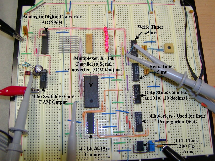
ADC 0804 and One Shot Timers |
| This circuit takes an analog signal and converts it to a digital serial bit stream. The circuit starts with a clock pulse of 5 ms (milliseconds). A 555 timer chip is used to create a TTL, 0 - 5 Volt square wave clock pulse. The clock signal is fed into the 74193 counting chip. The 4 - bit counter can count up to 1111 in binary, 0 - 15 in decimal. The 7408 AND gate is across the counter's output D and B therefore setting the counter when it reaches 1010 or 10 in decimal. The AND gate's output goes through four inverter gates before it connects to the clear pin of the counter. The reason for this is the Propagation Delay of the inverters delay the signal a few nanoseconds to allow the 74121 one shot timer to trigger. |
The One Shot is similar to the 555 timer where the timing cycle is based on the RC time constant, resistance * capacitance. The first one shot is used for the read cycle. When the 74193 counts to 10, the 5ms sample cycle is started. The ADC0804 is sampling the signal then it converts it into data bits. The ADC read and write pins are labeled as a processor would see them, ADC as a memory chip. Therefor, the read active low, actually writes data out of the ADC and a external processor would then read it. The read timer sends a low signal for 45 ms and a high signal for 5 ms. The high pulse turns on the PAM gate and feeds the analog signal into the ADC. The low pulse holds data on the ADC's 8 - bit buss.
|
74150 Multiplexer |
PCM NRZ and PAM |
|
During the output cycle, the ADC output of 8 - bits are converted to a single serial bit stream. The ADC is feed into the 74150 multiplexer to convert parallel to serial. The multiplexer has eight inputs. With each clock cycle, one input is read and sent to pin 10, the serial output of the 74150. After eight clock cycles, 40 ms, all the data is sent out. The timer is set to 45 ms. The left over 5 ms is used for embedded clock signal. The 74150 has 3 - bit address input from the 74193 counter. The address input is 000 - 111 which is 0 - 7 in decimal. This defines which of the eight data inputs will go out to the serial output pin 10.
|
PCM - Pulse code modulation is the output of the serial data stream using NRZ line coding, non-return to zero. This line code goes high to high without going low in between signals when the data stream has two high in a row.PAM - Pulse amplitude modulation is created with the 4066 switch. This switch conducts for 5 ms during the ADC read cycle. The analog signal enters the system through the 4066. The signal is chopped into 5 ms chunks and feed into the ADC 0804 where it is then sampled and converted into bits. |
Click Here for Timing Diagrams